India’s PCB Renaissance: How Govt Policy, PLI & Onshoring Are Fueling a Local Boom

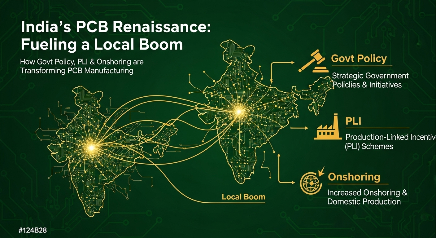
Over the past few years, India has been making bold moves to strengthen its electronics manufacturing sector. Backed by government schemes like PLI (Production Linked Incentives) and a broader push for onshoring critical components, the country is entering what many call a PCB renaissance.

For companies building smartphones, 5G networks, automotive electronics, and IoT devices, this shift means shorter supply chains, reduced import dependency, and greater local availability of advanced printed circuit boards (PCBs).


The Role of PLI and Govt Incentives

The Indian government has announced multiple programs to attract investment and boost electronics production. The PLI scheme, in particular, rewards companies that expand local manufacturing capacity while meeting output and export targets.

Key highlights include:

  • Incentives for large-scale electronics manufacturing and component ecosystems
  • Special focus on semiconductors, PCBs, and display units
  • Support for both domestic players and global companies setting up plants in India
  • Integration with “Make in India” and “Digital India” initiatives

This policy-driven growth is already visible. Several international electronics majors have announced plans to establish or expand operations in India, and local companies are scaling up to meet demand.


Why PCB Manufacturing is Critical

PCBs may not get the same attention as semiconductors, but they are just as essential. Every device — from a smartphone to a satellite — relies on them. Without a strong local PCB ecosystem, India’s electronics value chain remains incomplete.

Some reasons why PCBs are central to this ecosystem:

  • Base of all electronics: No electronic device functions without a reliable PCB.
  • Import dependency: Until recently, a large share of advanced PCBs was imported, mainly from East Asia.
  • Time-to-market: Local PCB manufacturing reduces lead times for Indian companies.
  • Cost efficiency: Domestic sourcing cuts logistics costs and currency risks.
  • Security & supply chain resilience: In critical sectors like defense, space, and telecom, local PCB production improves strategic independence.

Impact on Imports, Supply Chains & Global Partnerships

As India ramps up PCB production, the ripple effects are clear:

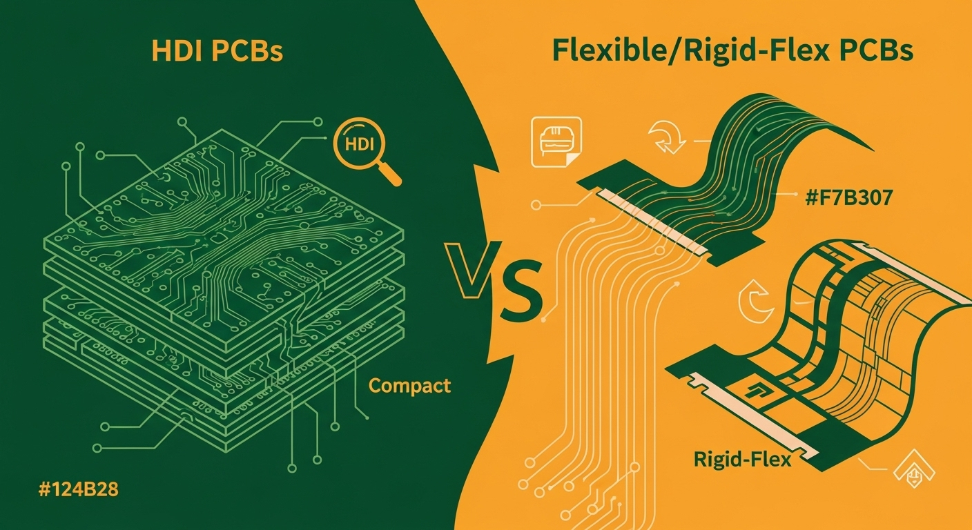
  1. Reduced Imports: A stronger domestic base reduces reliance on imports, especially for multilayer, HDI, and rigid-flex boards.
  2. Improved Supply Chains: Local manufacturing ensures faster turnaround and quicker prototyping for startups and OEMs.
  3. Global Collaboration: With incentives in place, global firms are more open to partnerships, joint ventures, and technology transfers.
  4. Export Potential: As capacity scales, India can position itself not just as a consumer market but as a global hub for PCB manufacturing.

Where Sulakshana Circuits Fits In

At Sulakshana Circuits Limited (SCL), we see this as both an opportunity and a responsibility. Since 1988, we have been part of India’s journey in electronics manufacturing, providing reliable, high-quality PCBs for industries ranging from telecom and defense to automotive and consumer electronics.

Here’s how we align with this new wave:

  • Technology Readiness: From ROHS-compliant boards to ENIG finishes, HDI, and exotic substrates like Rogers, our capabilities match the requirements of next-gen applications.
  • Quick Turnaround: Our commitment to on-time delivery supports India’s growing ecosystem of startups and global OEMs who demand faster design-to-production cycles.
  • Sustainability: As environmental norms tighten, SCL is actively investing in greener processes and exploring renewable PCB materials for the future.
  • Scalability: With decades of experience, we are positioned to scale alongside India’s expanding electronics ecosystem and global supply chain integration.

The Bigger Picture: India as a Global PCB Hub

The next five years could see India become one of the world’s largest electronics manufacturing centers. With demand soaring for 5G devices, EV components, IoT hardware, and medical electronics, the importance of reliable PCB suppliers will only grow.

Companies that invest today in local partnerships and manufacturing capacity will be best placed to benefit from:

  • A rapidly growing domestic market
  • Strong government support through PLI and related policies
  • Opportunities to export to global markets seeking alternatives to single-source supply chains

Conclusion

India’s PCB industry is entering a new era. Backed by PLI schemes, government incentives, and rising demand across sectors, local manufacturing is poised to reduce import dependency and strengthen supply chain resilience.

For innovators, this means faster access to high-quality boards. For manufacturers, it opens the door to global partnerships and exports.

At SCL, we are proud to be part of this transformation. With more than three decades of experience, we continue to adapt, innovate, and deliver PCB solutions that support India’s growing role in the global electronics ecosystem.

Sustainability & the Next-Gen PCB: Recyclable, Renewable & Reconfigurable Boards

Sustainability has become one of the defining challenges in electronics manufacturing. As consumer demand for greener products grows and regulations tighten across industries, printed circuit boards (PCBs) are coming under closer scrutiny.

Traditionally, PCBs have relied on FR4 substrates, copper, and epoxy resins — materials that are durable but difficult to recycle. The result is a growing mountain of electronic waste worldwide. In 2025, new approaches such as biodegradable substrates, recyclable laminates, and substrate renewal technologies are reshaping how PCBs are designed and manufactured.


Why Sustainability Matters in PCB Manufacturing

Electronics account for a significant share of global waste. According to recent studies, millions of tons of e-waste are generated each year, and PCBs make up a large fraction due to their complexity. Unlike plastics or metals, PCBs are multi-material composites, making them hard to recycle at scale.

This is where innovation is changing the game. New research and industrial practices aim to create recyclable PCBs, renewable substrates, and processes that minimize waste, while still meeting the performance requirements of modern electronics.


New Materials for Sustainable PCBs

Several promising materials are moving from labs to production lines:

  • Biodegradable Substrates – Polymers such as polylactic acid (PLA) or natural fibers can be used to create circuit bases that break down after disposal, reducing landfill impact.
  • Water-soluble PCBs – Concepts like DissolvPCB use polyvinyl alcohol (PVA) substrates that dissolve in water, leaving behind reusable components and copper.
  • Liquid Metal Conductors – Materials such as gallium-based alloys are being tested as alternatives to traditional copper. These offer potential recyclability and unique electrical properties.
  • High-temperature, eco-friendly laminates – Alternatives to conventional FR4 that meet RoHS standards and reduce the use of harmful flame retardants.

Techniques Like “PCB Renewal”

Instead of discarding the entire board at end-of-life, some manufacturers are exploring PCB renewal methods. The idea is simple:

  • Reuse the substrate by stripping off existing components and copper layers
  • Reapply new layers for a fresh design
  • Extend the lifecycle of the same base material, reducing raw material demand

This approach may lower costs in the long run while addressing e-waste concerns. Though still in development, PCB renewal could complement recycling in high-volume industries such as consumer electronics and automotive.


Lifecycle and Cost Trade-offs

Sustainable PCBs must balance eco-friendliness with performance and cost.

  • Lifecycle Benefits: Green PCBs reduce landfill waste and allow easier recovery of valuable metals like gold and copper.
  • Cost Factors: Biodegradable or recyclable substrates can be more expensive to produce today, but as adoption scales, costs are expected to fall.
  • Design Challenges: Engineers need to ensure that new materials meet the same reliability standards as traditional FR4, especially for high-frequency or high-temperature applications.

For many manufacturers, the key will be gradual adoption: combining proven processes like RoHS-compliant finishes with pilot projects in renewable materials.


What Sulakshana Circuits Can Do

At Sulakshana Circuits Limited (SCL), sustainability has always been a part of how we think about PCB manufacturing. While our focus has been on RoHS compliance, ENIG finishes, and reliable quick-turn production, we see sustainability as the next major leap in the industry.

Some ways SCL can contribute include:

  • Partnering with material innovators to test eco-friendly laminates and biodegradable substrates
  • Exploring waste reduction in plating and etching processes
  • Adopting renewable energy for manufacturing facilities
  • Offering clients greener alternatives for specific applications, particularly in IoT, medical devices, and consumer electronics

By combining experience with new research, we can help our customers meet both performance requirements and environmental goals.


The Future of Green PCBs

Sustainable PCB manufacturing is no longer just a research project; it is becoming a strategic requirement for electronics companies worldwide. Governments are introducing stricter e-waste regulations, and consumers are increasingly aware of the environmental footprint of their devices.

The next generation of PCBs will not only be smaller and more powerful but also smarter in how they are made, used, and reused. From recyclable boards to renewable substrates and substrate renewal, the industry is moving towards a future where PCBs contribute less to waste and more to circular manufacturing.


Conclusion

The move toward recyclable, renewable, and reconfigurable PCBs is reshaping the industry. While challenges remain in cost and material reliability, the direction is clear: sustainability will be a core design requirement in the coming years.

At SCL, we are committed to staying ahead of this trend, helping our customers choose PCB solutions that are not only technically advanced but also environmentally responsible. By working together, manufacturers and innovators can ensure that the electronics of tomorrow are both high-performing and sustainable.

HDI vs Flexible/Rigid-Flex PCBs: Choosing the Right Technology for 5G, Wearables & IoT in 2025

Printed circuit boards (PCBs) form the foundation of every modern electronic product. As devices get smaller, faster, and more feature-packed, traditional PCB designs often fall short. Two technologies that have become especially important in recent years are HDI (High-Density Interconnect) PCBs and flexible or rigid-flex PCBs.

Both serve different purposes, and understanding their strengths is critical when designing products for fast-growing markets like 5G communication, IoT sensors, and wearable devices.


What is an HDI PCB?

An HDI PCB uses advanced manufacturing techniques such as microvias, finer traces, and higher wiring density to pack more functionality into a smaller footprint. This design approach allows engineers to fit complex circuits into compact products without sacrificing performance.

Advantages of HDI PCBs:

  • Higher component density for compact designs
  • Better signal integrity at high frequencies
  • Improved electrical performance with reduced crosstalk
  • Ideal for multilayer applications where space is limited

Typical applications: smartphones, 5G routers, tablets, aerospace systems, and high-performance computing boards.


What are Flexible and Rigid-Flex PCBs?

Flexible PCBs are built on materials that can bend, twist, or fold, allowing them to fit into unconventional shapes or moving assemblies. Rigid-flex PCBs combine rigid sections for component mounting with flexible sections that can fold, creating a hybrid design that saves space and reduces connectors.

Advantages of Flexible/Rigid-Flex PCBs:

  • Lightweight and thin, making them ideal for compact devices
  • Increased reliability due to fewer interconnects and solder joints
  • Ability to handle continuous bending and dynamic movement
  • Simplified assembly compared to multi-board solutions

Typical applications: wearable devices, medical implants, cameras, automotive electronics, and defense equipment.


HDI vs Flexible/Rigid-Flex: A Practical Comparison

Feature/FactorHDI PCBFlexible/Rigid-Flex PCB
Size & DensityVery high density, compact multilayerModerate density, optimized for form factor
FlexibilityRigid, not bendableCan bend, twist, and fold
Signal IntegrityExcellent for high-speed signalsGood, but design must consider flex movement
DurabilityStrong under static useStrong in dynamic or moving environments
CostHigher than standard PCBs, cost-effective in volumeMore expensive due to material and complexity
Best Use Cases5G devices, computing, aerospaceWearables, IoT sensors, medical devices

Which One Fits 5G, Wearables, and IoT?

  • 5G Devices
    HDI PCBs are the go-to choice. With their ability to handle high-speed signals, reduced loss, and compact design, they are perfectly suited for the tight layouts of 5G smartphones, routers, and small cells.
  • Wearables
    Flexible and rigid-flex PCBs dominate this space. Devices such as fitness trackers, smartwatches, and medical monitoring equipment rely on boards that can bend and survive constant movement.
  • IoT Sensors
    Both technologies have a role here. HDI PCBs are useful for high-performance IoT gateways or compact communication modules, while flexible PCBs are ideal for lightweight, portable sensors deployed in varied environments.

Key Considerations When Choosing

  1. Space and Size Constraints
    If every millimeter matters and your design is dense, HDI may be the better choice. If the product requires bending or folding, flexible PCBs win.
  2. Performance Requirements
    For high-speed, high-frequency applications like 5G and data centers, HDI is superior. For wearables or medical devices where comfort and adaptability are more important, flex PCBs are ideal.
  3. Cost Factors
    Both HDI and flexible PCBs cost more than standard boards, but the trade-off is improved performance and reliability. Early planning with your PCB manufacturer helps balance cost and design requirements.
  4. Reliability in the Field
    HDI PCBs excel in stable, compact environments. Flexible and rigid-flex PCBs are more reliable in applications involving motion, vibration, or irregular shapes.

The Role of PCB Manufacturers in 2025

With India’s growing electronics ecosystem and global demand for advanced boards, choosing the right manufacturing partner is just as important as the technology itself. At Sulakshana Circuits Limited (SCL), we have over three decades of experience in delivering advanced PCB solutions. Our expertise covers ROHS-compliant PCBs, HDI designs, ENIG finishes, and flexible/rigid-flex solutions tailored to high-performance applications.

Whether you’re developing a 5G device, a new IoT solution, or a next-gen wearable, working with an experienced PCB manufacturer ensures your design moves smoothly from prototype to production.


Conclusion

The choice between HDI and flexible/rigid-flex PCBs depends entirely on the product requirements. For high-density, high-speed designs, HDI PCBs provide unmatched performance. For lightweight, compact devices that require flexibility, rigid-flex and flexible PCBs are the way forward.

In 2025 and beyond, both technologies will continue to drive innovation in 5G networks, IoT ecosystems, and wearable electronics. By understanding their differences and working with a trusted manufacturing partner, engineers can build products that are efficient, reliable, and future-ready.